I agree my information will be processed in accordance with the ENSEMBLE³ Privacy Policy.
Sign up for our newsletter
I Privacy policy |
Functional Materials Technology Group
Optical Nanocharacterization Group
Inverse Materials Design Group
Next-Generation Energy Systems Group
Biophotonic Applications Group
Solar Energy Conversion Group
Oxide Single Crystals Group
A3B5 Compound Semiconductors Group
Functional Materials Laboratory
Oxide Single Crystals Laboratory
Materials Characterization Laboratory
III-V Compound Semiconductors Laboratory
Contact
Ensemble3 sp. z o.o.
01-919 Warsaw
133 Wólczyńska St.
NIP 1182211096
KRS 0000858669
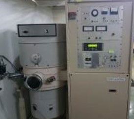
Sputtering SYSTEM ULVAC SBR-230 6E (Ł-IMiF)
A system for the application of polycrystalline and amorphous layers by the sputtering method. It has the possibility of deposition directly from targets (possibility of applying multi-component targets) and the so-called reactive sputtering of gases in reactive atmospheric layers of conductive and non-conductive materials. There is also the possibility of re-cleaning substrates before the layer application process. The size of used substrates is in the range from 5 x 5 mm to 100 x 100 mm and thickness from 0.05 mm to 50 mm.


